hoursminutes
per batch
-CvRJYGY4.svg)
TRACE turns microscope images into thousands of automated, pixel-precise measurements. Starting with PCB cross-sections.
Today, engineers measure cross-sections by hand: a few clicks per layer, hours per batch, and results that depend on who is at the microscope. TRACE measures every layer boundary automatically.
per batch
measurement points per layer
same image, same consistency, every time
boundary detection on every layer
Drop in a microscope image of your cross-section: PNG, JPG, TIF or BMP
µm per pixel typed once, or read from the file name
Using in-house computer-vision model, TRACE finds every layer boundary and classifies materials: copper, substrate, plating, HASL.
Thousands of measurements per layer for consistent, pixel-precise results
Per-layer statistics (mean, min, max, percentiles, standard deviation) in an IPC-ready export. Dense, consistent data you can defend in any audit.
| layer | dir | mat. | min µm | mean µm | max µm | n | |
|---|---|---|---|---|---|---|---|
| 1 | V1 | vert | Cu | 21.00 | 41.11 | 45.00 | 339 |
| 2 | H1 | hor | dielectric | 98.00 | 112.40 | 126.00 | 284 |
| 3 | V2 | vert | Cu | 12.00 | 13.86 | 17.00 | 381 |
| 4 | H2 | hor | dielectric | 84.00 | 96.52 | 108.00 | 271 |
| 5 | V3 | vert | Cu | 13.00 | 14.38 | 17.00 | 380 |
| 6 | H3 | hor | dielectric | 102.00 | 118.70 | 134.00 | 296 |
Fits your existing setup without any expensive new hardware
Production images stay on-site
Nothing is stored by us
Simple local installation
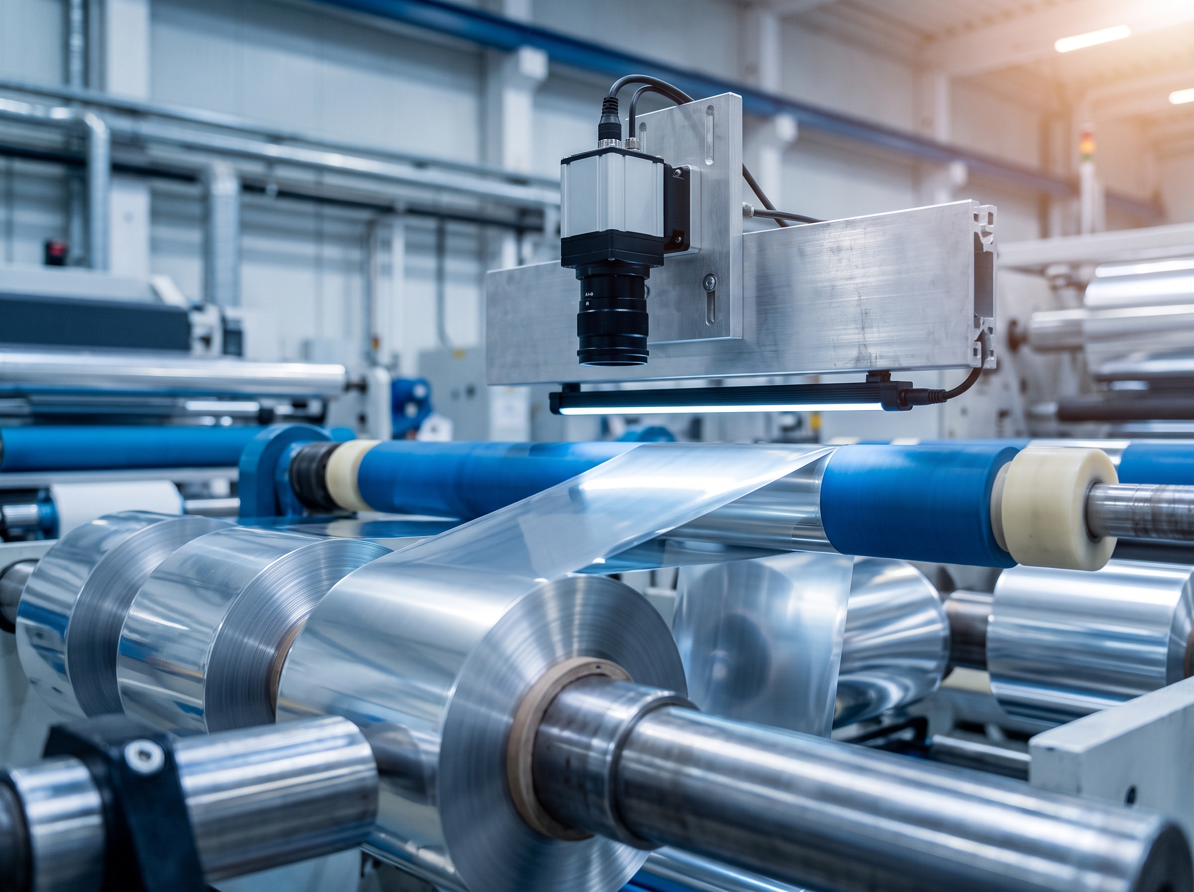
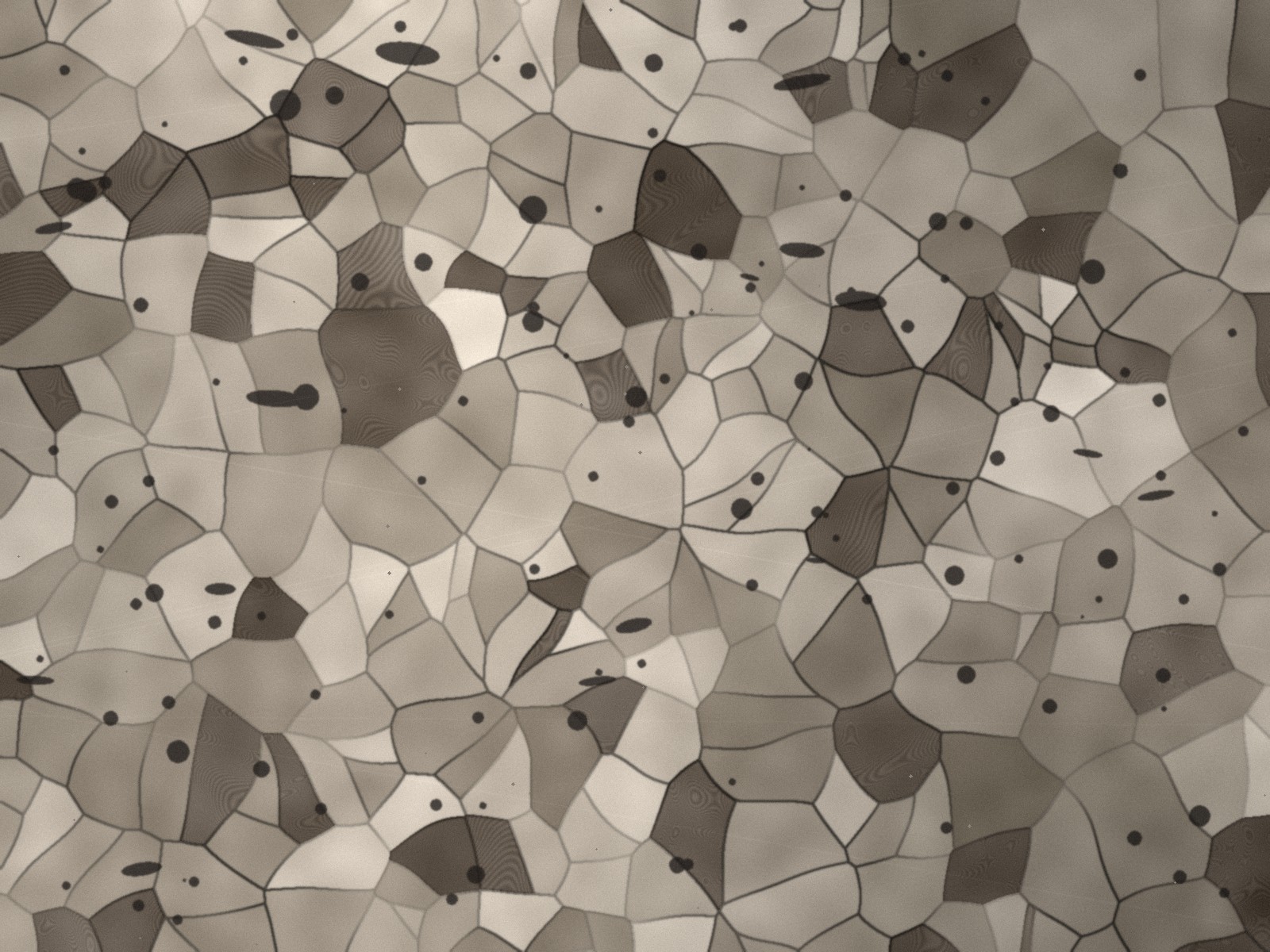
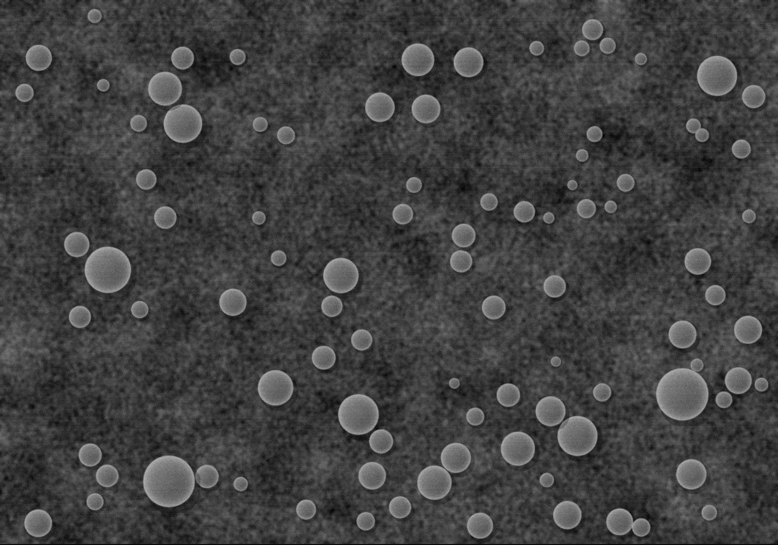
Our core is a precision boundary-detection model for microscopy images. PCB cross-sections are where we start. The same measurement problem exists across materials and industries.
We are currently piloting TRACE with Finland’s largest PCB manufacturer, Aspocomp, and we’re onboarding a limited number of new pilot partners.
 PCB MANUFACTURER · FINLAND
“TRACE has significantly simplified and accelerated parts of the inspection workflow.”
Paraphrased from verbal feedback during an Aspocomp meeting. Not a quantified performance benchmark.